

I never expected much from a Nintendo alarm clock, but Alarmo pushes all the wrong buttons for me, and I've hated it since day one.
First, the pros are that it's easy to set up, the interface is simple, the sounds are fab, and the sleep tracking is excellent. New music is being added over time, too!
But for me, that's where it ends. But the thing is, my Apple Watch can do all of that anyway, as can my iPhone. Additionally, it's fidgety having to stop and alarm (which I guess is the point), and it's made more fidgety by being on my bedside table and not responding to my voice (again, maybe the purpose of such a device is to do this). Next, the fiddly button on the top. Why not just add a touch screen? WiFi was particularly frustrating to do on this control stick.
For now, my Alarmo will go away into a cupboard, and I will likely set it up in the spare room when guests come round. It no longer feels right having this wake me in the morning alongside my HomePod.
This thing is a waste of money, even if you're a Nintendo fan like me!
We’ve gone full circle in UI design. What began as the richly tactile skeuomorphism of early smartphone interfaces gave way to the clean simplicity of flat design, only to reincarnate as the soft shadows of neumorphism—and now we find ourselves embraced by a new "glass" look. With Apple’s recent introduction of their frosted-glass style effect, it’s clear that designers are once again drawing inspiration from the physical world, layering translucency, depth, and context to bring digital surfaces to life.
From leather stitching to simple borders
In the late 2000s and early 2010s, skeuomorphic interfaces reigned supreme. Buttons looked like real buttons, notes looked like yellow legal pads, and readers flipped virtual pages in the Newsstand app. The goal was familiarity: to help users learn digital tools by evoking real-world metaphors.
But by 2013, Apple’s iOS 7 heralded a new era. Shadows vanished, textures flattened, and colours brightened. Suddenly, interfaces felt more abstract—icons became simple glyphs, and grids and cards organised content with minimal ornament. This "flat design" philosophy prioritised clarity, performance, and scalability, influencing everything from Android’s Material Design to countless web and desktop applications.
Neumorphism
Fast-forward to around 2020, and designers began craving warmth and tactility within flat layouts. Enter neumorphism—a style that married flatness with subtle, extruded shadows. Elements appeared as though gently raised or inset into the background, lending a sense of touchable realism without reverting to literal material textures.
While visually striking, neumorphism proved challenging for accessibility. Low contrast between elements and backgrounds sometimes made interfaces hard to navigate, and the delicate shadows could feel more decorative than functional.
Glassmorphism
Now, we're witnessing a resurgence of layered translucency with Apple’s freshly unveiled frosted-glass effect (first glimpsed in their latest OS previews). Unlike skeuomorphism’s heavy textures or neumorphism’s tonal embossing, glassmorphism leverages blur, light, and colour bleed:
- Depth & Context: Background content subtly shows through translucent panels, reinforcing spatial relationships without overwhelming.
- Focus & Hierarchy: Blurred backdrops push primary controls and information into sharper relief, guiding user attention naturally.
- Modern Nostalgia: The effect nods to Windows Aero’s “glass” of the late 2000s while feeling fresh thanks to Apple’s refined blur algorithms and dynamic colour adaptation.
In practice, glassmorphism offers both form and function: you see hints of underlying content (context preserved), but the blur ensures legibility and focus. Apple’s implementation dynamically adjusts tint and translucency based on ambient lighting and on-screen content, creating a living, responsive canvas. This is rare in modern UIs.
So where are we now?
Design trends rarely die—they evolve. Skeuomorphism taught us the power of metaphor; flat design taught us clarity and efficiency; neumorphism reminded us of dimensionality; and glassmorphism now balances all three, marrying context, aesthetics, and usability.
This cyclical return speaks to a more profound truth: users crave interfaces that feel both intuitive and alive. Pure flatness can feel cold, and overly literal textures can feel gimmicky. However, translucent layers create interfaces that are simultaneously minimal and rich, echoing how we perceive real glass.
We should expect that push to continue, with more skeuomorphic elements and interfaces creeping back into our everyday life, and I'm not happy!
When I first started blogging in 2009, I was asked if HDMI could accept input and output over the same connector (not precisely at the same time). Of course, a graphics card with an HDMI port on it is most likely only for video output and not video input. Of course, the answer, therefore, was no.
But why not?
Well, the answer is that it's just not been implemented. That's because HDMI was never designed this way. Usually, when a connector (such as USB-C) is bidirectional, a handshake protocol is implemented that decides the connector's data flow.
Some features of HDMI, like Audio Return Channel (ARC) and Consumer Electronics Control (CEC), are, of course, bidirectional; for CEC, for example, the device can control a TV, and the TV can also control the device, and for ARC, the audio can be sent back to the device.
As games become increasingly demanding, the need for advanced hardware grows. Back in 2009, I had a Radeon 5670, a mid-range graphics card, which allowed me to run most triple-A titles at moderate settings. This was sufficient at the time, but as my interest in PC gaming grew, I wanted to play all my triple-A games on my PC. Consequently, I upgraded to a Radeon R7950, AMD's second-best card at the time, which could effortlessly run triple-A titles at full settings in 1080p.
However, the R7950 struggles with any modern titles at 1080p today, such as Warcraft 3 Reforged and Forza Horizon 4, due to its now modest 3GB of VRAM. Most contemporary graphics cards come with at least 8GB of VRAM, which is now considered the minimum for playing modern 1080p games at moderate settings.
Despite 1080p not being a high resolution by today's standards, running games with demanding graphics still requires significant processing power and VRAM. Even at 1440p, some computers with 8GB of VRAM struggle to handle the latest titles because of their high demands. The rise of technologies such as ray tracing and more detailed textures has only amplified these requirements, pushing even mid-range systems to their limits.
In summary, while 8GB of VRAM should suffice for 1080p gaming at high or ultra-high settings for some games, it falls short for 1440p gaming or higher at those settings, especially with high refresh rate displays (though VRAM does not directly impact refresh rate). For 4K gaming, I believe a minimum of 16GB of VRAM is necessary, regardless of the settings.
The rapid evolution of game graphics and performance demands has made it crucial for gamers to continually upgrade their hardware to fully enjoy the latest titles. This trend also raises questions about the sustainability of gaming habits and the financial burden of keeping up with technology.
I aim to spark a discussion on this topic and would love to hear your thoughts. Please send me an email or reach out via my website. Your insights and experiences with hardware upgrades and gaming performance would be invaluable to this conversation. Let’s explore together how we can best navigate the ever-changing landscape of PC gaming.
It was slightly disappointing when I went into teacher training to discover that the course had been named Computing Science rather than Computer Science. The two have different meanings, and what we teach is called Computing Science, but it is actually Computer Science.
Computing science is generally associated with computer science's theoretical and mathematical underpinnings, where logic gates and formal specification are prominent. On the other hand, computer science is more related to designing and developing algorithms and using and creating data structures, computational thinking, computer programming, computer architecture, databases and data storage, HCI/UX and much more.
So, to answer the question I was asked the other day about whether Computer Science (at the university) is the same thing as Computing Science (in school), I answered yes, but knowing that this was only in this context. I am absolutely not being pernickety here as I genuinely think that the difference between these two disciplines is essential to distinguish.
Enough said, really.
Tim Berners Lee, the man considered the father of the web, conceptualised the idea back in 1980, but it wasn't until 1989 (two years before I was born) that he came up with the solution we now know as the web.
Berners Lee suggested combining hypertext and the Internet for document sharing back then. Now, the web has become far more than this and, coupled with the Internet, has become a superhighway of information.
The trend of smartphones replacing functionality that was once carried out by a desktop or laptop computer is continuing to grow. With companies like Samsung and Google at the forefront of this new technology, things like DeX, we are beginning to see a new bring-your-own-device to work scenario growing. A lot of this functionality has come from the latest chips being powerful enough to perform desktop-like functions and give a desktop-like environment without struggling but it's also down to the advancements in cable technology like USB Type C and its Alt-Mode function.
Let's look at the first point made here: smartphone chips are more powerful than ever, boasting up to 6GB or 8GB of RAM and decent graphics processors. They are more than capable of running Windows 7 based on those specifications, so they are more than capable of running your desktop applications such as Microsoft Word in a smartphone form. Microsoft attempted to do this with their phones using Continuum [1]. This was a fairly wild idea back in 2015 when smartphone processors were nowhere near what they are now. But this kind of thing is now very possible for the average job (we're not talking about playing games on a secondary display with a mouse and keyboard) such as Microsoft Word or PowerPoint. I can see this being very useful for me if I was doing another talk where I could simply dock my phone rather than my laptop. Apple has now made this possible on iPad with the new Stage Manager feature which is very impressive - this kind of thing should come to iPhone when docked.
Now let's look at the second point made here, connectivity. Connectivity is perhaps the main reason this kind of stuff is becoming very possible. Looking at what Microsoft was trying to achieve in 2015 with micro USB (which by the way, was USB 2.0) and USB Type C (later on, however). This is a great idea, one that I fully support. Samsung's DeX feature is actually so seamless that a company my brother was working at during a contract with some 200+ employees in the part he was working at had moved to bring-your-own-device and they would dock it into their USB Type C docks to connect the corporate network and gain a mouse, keyboard and display. Not only does this save the company money, but it also reduces the number of devices the users actually need, adds functionality such as making phone calls from their desktop system and perhaps the most interesting one is that it can actually be used to reduce the amount of time users spend on non-work related apps on their phones (users can enable a work mode when the phone is docked, allowing them to only use work-related apps).
Now some say that the future of smartphones taking over laptops is well away [2], and sure I can definitely agree, but when I heard a whole 200+ people were using their phones using Samsung DeX as their sole working device, I was absolutely astonished. Sure where I work we've done away with desktops, your laptop simply connects to the keyboard, mouse, 2 displays and projector by docking with USB Type C, but it's not quite the same as replacing a laptop with a smartphone or even a tablet for that matter.
[1] https://www.theverge.com/2015/4/29/8513519/microsoft-windows-10-continuum-for-phones
[2] https://www.teamtreysta.com/will-smartphones-take-over-laptop-functions-in-the-future/
The website repl.it is provides an online code editor that features tons of great tools to assist in development. Schools across Scotland rely heavily on the website, and materials created refer to repl.it over and over, including those from large groups that make materials available for teachers in Scotland.
But this is an issue.
By depending on repl.it and putting all your effort into the platform, you are investing heavily in an organisation that seeks to make money and who may in turn decide to make educational benefits non-existent. This happens all the time: JetBrains did this, removing and changing their educational discounts (and going from offering free packs of their software to charging the full amount).
Secondly, and perhaps more important to me as a computing teacher, is that by teaching pupils to use repl.It, we are teaching them one environment for developing software, when we should be teaching them things that are used in the industry, such as IDEs like VS Code or Atom. This frustrates me as someone who has worked in the industry for a few years prior to becoming a teacher because I know no one uses repl.it where I've worked. It's a bit like teaching someone to drive a Ford Focus by telling them where everything is in that car and then expecting them to know how to drive a bus after passing their test. Don't teach them one thing; teach them the general skills that apply to all of them.
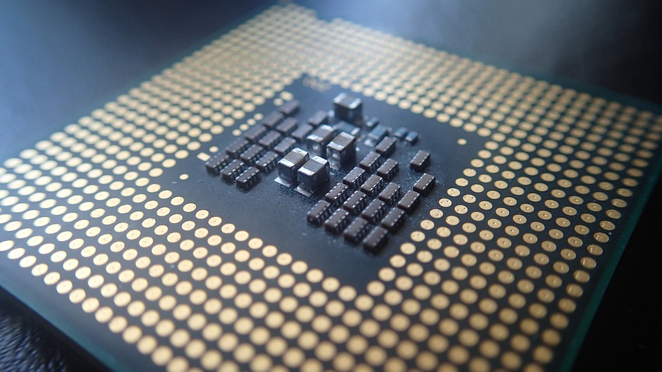
Moore's Law was kind of like the golden rule for computer systems. Developed by Intel cofounder Gordon Moore, the rule has been the centrepiece and fundamental principle behind the ever-improving computer systems we have today. It basically spelt out the future in that computers will get better performance year after year (doubling in performance, roughly).
It did this by not increasing the package size of the CPUs but by reducing the feature size. Take my EliteBook for example. It has a Ryzen 6850U processor, built with a 7-nanometer process. This 7-nanometer process is called fabrication, and it roughly means that the size of each transistor within a package (a CPU die) is around that size. The smaller and smaller the feature size the more and more likely it is for something to fail or go wrong during production, making it more and more difficult to manufacture CPUs as the feature sizes get smaller. Not only that, it has always been said that we will be unable to get the feature size smaller than the size of an atom (which is approximately 0.1 nanometers in size). The theoretical boundary for the smallest feature size that we can manufacture is approximately 0.5 nanometers - that's not that far away from where we are at 4 nanometers in 2023.
Over the last few years, manufacturers have been trying to squeeze every bit of performance increase out of the latest chips. Apple has been increasing the physical size of the processors by adding several chips together (think of the M1 Pro and Max which are simply M1 chips stuck together with a little bit of magic). This makes the processor very large and unsuitable for smaller devices. AMD, on the other hand, has moved to a design where wastage is less frequent thus increasing the yield of good processors and in turn allowing them to cram more performance into their dies.
To combat such an issue, the manufacturers of some CPUs moved to a chiplet design. This chiplet design is basically where several components such as the memory controller, IO controllers such as USB and so on compared with the original monolithic architecture used in the past. The first time I experienced a chiplet-based CPU was the Intel Core 2 Quad, where it was literally two Core 2 Duo dies on one chip. The issue is that it takes more space than building a chip using a monolithic architecture where the entire processor resides within one die. There are also other complications such as communication internally between these dies, but they can be easily overcome once it's been done with one chip, as the designs can continue to be used in other chips. There are also power consumption concerns when two CPU dies are put on the same chip, but with chiplets for IO and memory, this actually reduces the distance between the CPU and the chip, thus actually reducing power consumption and increasing performance. Chiplet design also keeps costs down as it reduces binning a good processor when a section of it fails. For example, if all IO was built into the actual CPU die (as is the case in a monolithic architecture) and only one part of the IO section failed, the whole processing unit would be binned. With a chiplet design, if there is a failure in the IO section, it happens only in that chiplet - a much less costly fix as all it would require is a replacement IO die.
Another way manufacturers are continuing to squeeze performance out of these chips is by embedding algorithms in them. This has always been a feature of CPUs since the Pentium MMX which brought several instruction sets to improve the multimedia capabilities of computers back then. It basically means that instead of a programmer writing an algorithm say to do the vector encoding using something like AVX-512, the CPU does not need the user to write the program. The program is actually an instruction built into the CPU and therefore it runs much faster. This is called hardware encoding. You'll see that Apple has done a lot of this in their M1 and M2 chips over the years to give them an even better performance result than the Intel CPUs they replaced. By doing this, Apple has managed to improve the effectiveness of its software through the use of hardware. This is actually something that could become a problem, however, and it might damage the cross-compatibility of software that can run on any operating system and any platform. I say this because if a piece of software is developed to use AVX-512 it's very likely that it will work on a system without AVX-512 instructions. But with an instruction being built-in such as one which utilises libraries specific to a GPU or CPU feature, cross-compatibility may not be possible without writing massive amounts of additional code (for example DirectX or Metal on macOS both cause issues when porting).
I have always believed since I was a teen that the second method is indeed the way forward, but it really would only work in a single CPU/GPU architecture world, a bit like if everyone was using x86. That's never going to happen, but perhaps if we had a library (Vulcan) that could abstract over those underlying APIs or hardware and make things simpler for developers, then maybe this is actually the best option.
Let's be honest here, Microsoft has been trying to ditch Control Panel since Windows 8 back in 2012, and yet here, all the way in Windows 11, 10 years later, Control Panel still resides in the core of the operating system. It's uses may have slowly begun to disappear, yet still there are so thing you can only do within Control Panel.
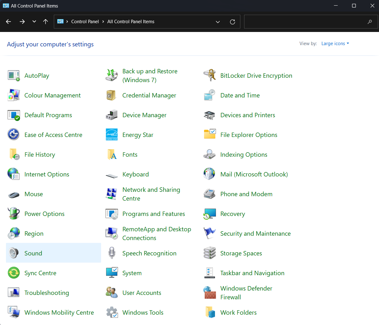
Windows 11 is still a mess with it's settings being spread across the whole system.
For example, to change the mouse double click speed, one must go to Control Panel and then the Mouse setting. There's other weird things in here such as the Work Folders feature, the Sync Centre (which should be a separate app in my opinion), AutoPlay, the Windows Mobility Centre (why does this still even exist?!), Windows Defender Firewall. But the worst of all, is the Programs and Features. Not knowing how to uninstall an app will confuse some people. The Mail feature is another weird one as well as Phone and Modem (that should have been removed from Control Panel a long time ago).
So why do these things still exist? Does Microsoft not care about making the OS perfect anymore?